Reverse Engineering of PCB Designs
CADX Design is a PCB design service bureau that has years of experience in designing printed circuit boards and schematic capture. We have extensive experience using CAM350 and other gerber manipulation tools to reverse engineer PCB designs and recapture lost PCB designs. We've been using CAM350 for a several years, up to the most current version of CAM350 available.
Our designers are experienced in schematic capture, PCB design, capturing component symbols, pattern creation, component creation, library management. The engineering experts at CADX Design are skilled in the conversion of PCB designs, electronic schematics, and netlist formats; we regularly employ these skills to not only convert between differing design formats, but also to reverse engineer PCB designs.
In addition, if you have corrupted gerbers or a corrupted aperture table, send us your data! In many of the cases where clients sent us corrupted gerber data, we were able to clean it up so that it could be read and understood by any standard gerber manipulation tool.
The following images are some examples of some PCB designs processed to gerbers and loaded into CAM350. They are shown here to give you a feel for the CAM350 interface.
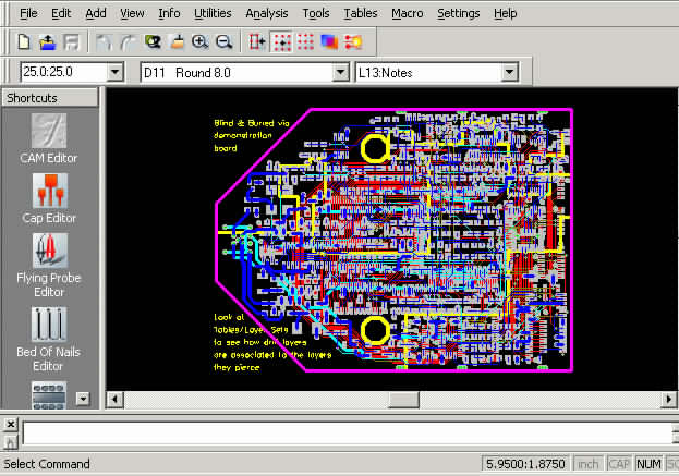
Sample Gerbers Loaded Into CAM350
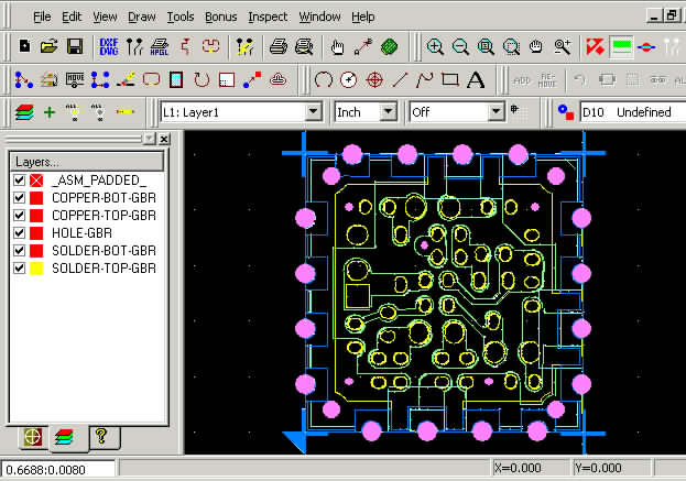
Sample Gerbers Loaded Into CAMtastic 2000
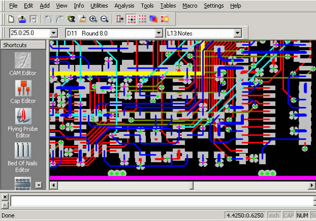
Sample Gerbers Loaded Into CAM350
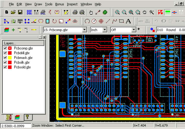
Sample Gerbers Loaded Into CAMtastic 2000